



EasyEDA Agent Connector
EasyEDA Agent Connector
zhoushoujian66EasyEDA Agent Connector
面向 EasyEDA(嘉立创EDA专业版)的 AI 原生自动化连接器。
easyeda-agent 把官方 EasyEDA 扩展 API 变成一套有类型、可观测、Skill 友好的系统。这个连接器插件本身保持很薄:它只负责连接本地 easyeda-agent daemon,并把 typed actions 分发到官方 eda.* API;真正的工作流、校验、确认、产物处理和多步编排,都在 Go CLI/daemon 与 Skill 层完成。
Skill / CLI -> Go daemon -> EasyEDA Agent Connector -> official eda.* API
- GitHub 仓库:https://github.com/zhoushoujianwork/easyeda-agent
- 安装脚本:https://raw.githubusercontent.com/zhoushoujianwork/easyeda-agent/main/install.sh
效果演示
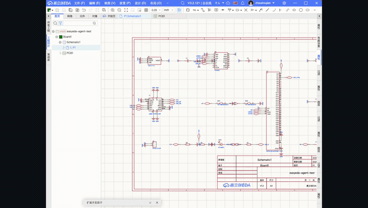
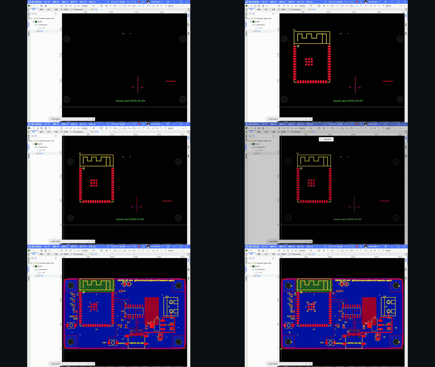
下面两段录屏来自真实 EasyEDA 画布:AI 从空白页开始生成原理图,再切到 PCB 完成布局、板框、铺铜和丝印。它不是生成一张图片,而是在编辑器里一步步执行 typed actions。
原理图从空白页生成:
PCB 布局与铺铜:
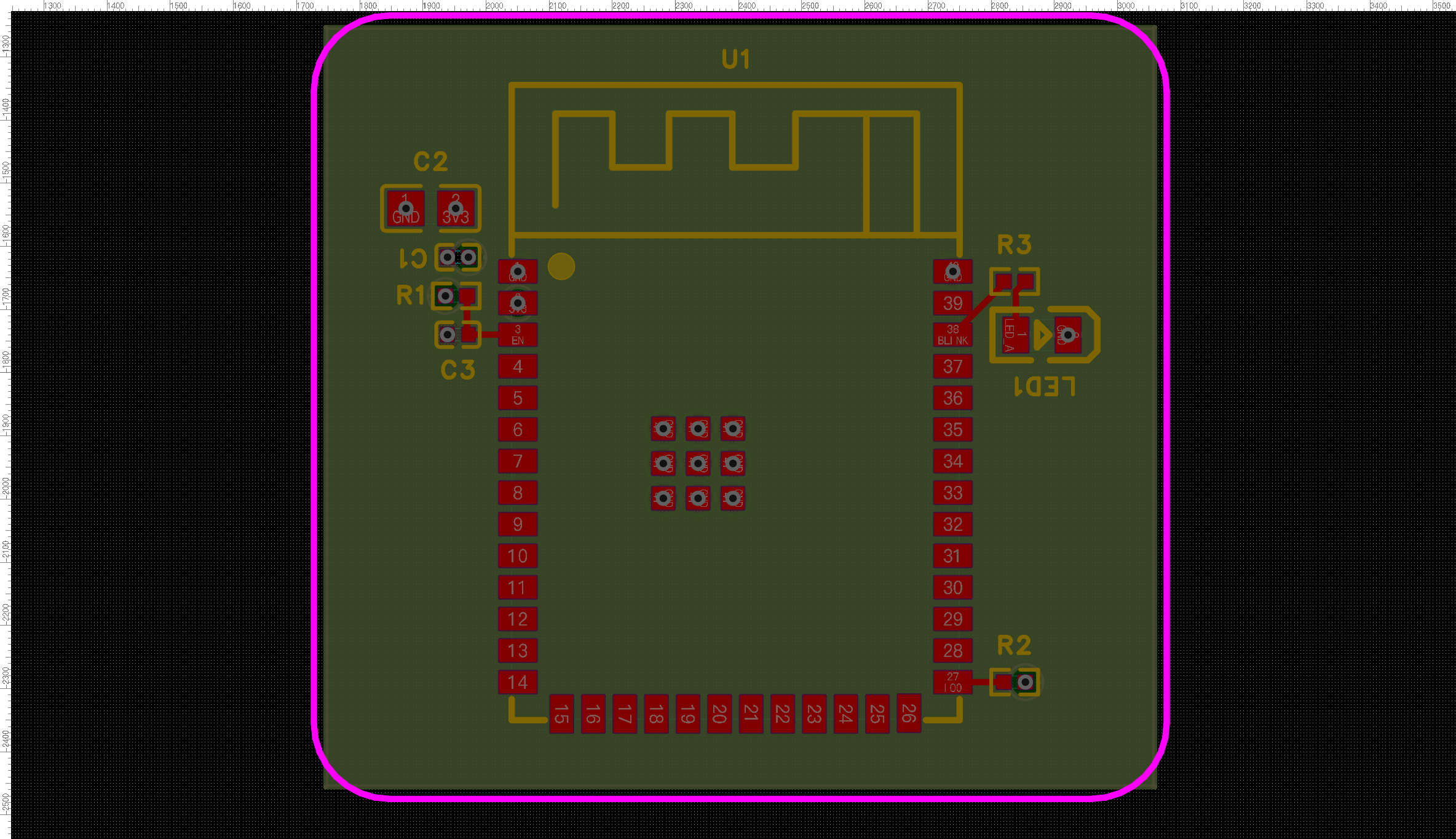
下面这块板由 agent 驱动完整 PCB 流程产出:自动布局 -> 板框贴合 -> 规则感知布线 -> 4 层电源平面 -> 丝印碰撞避让,并在真实 EasyEDA 画布上验证。
它是什么
这是一个真实可打包、可导入的 EasyEDA Pro 扩展。它桥接本地 easyeda-agent Go daemon 与官方 eda.* API,并且是整个系统中唯一直接调用 eda.* 的组件。
它主要负责:
- 本地 WebSocket 传输:端口扫描、握手、注册、上下文同步、心跳、自愈重连。
- typed action 分发:把 daemon 下发的结构化动作映射到官方
eda.*调用。 - 结果序列化:把执行结果、警告、错误、上下文回传给 daemon。
- 产物传输:把截图、BOM、网表等二进制结果编码后回传。
已支持的典型能力
- 原理图:放真实器件、布线、网络标志、选择、截图、DRC、BOM 导出、网表导出。
- PCB:新建板、导入、自动布局、板框贴合、铺铜、禁布区、叠层设置、截图、DSN 往返。
- 基础设施:自动重连、上下文感知、结构化错误、
debug.exec_js逃生口。
完整能力清单见 GitHub 仓库中的 docs/FEATURES.md。
安装
这个连接器只是薄桥接层,必须配套本地 easyeda CLI/daemon 一起用。
1. 装本连接器(两条通道任选):
- 在立创官方插件市场点击「安装」—— 平台可原地自动更新,最省心;
- 或从 GitHub Release 侧载
easyeda-agent-connector.eext—— 与 CLI 严格同版。
市场上架版本可能滞后于 CLI(当前市场约 v0.9.x,仓库已到 0.11.x)。四件套需严格同版时,请以 GitHub Release 里与 CLI 对齐的
.eext为准;市场版胜在平台自动更新,但可能落后。
2. 装 CLI/daemon 并启动:
curl -fsSL https://raw.githubusercontent.com/zhoushoujianwork/easyeda-agent/main/install.sh | sh
然后在 EasyEDA 中确认:
- 已安装本连接器(市场安装或
.eext导入)。 - 已开启「允许外部交互 / Allow external interaction」。
- 已启动本地
easyeda-agentdaemon。
完整上手、版本对齐与升级注意事项见 快速开始 & 使用注意事项 —— 四件套(CLI / 连接器
.eext/ Skill / EasyEDA)需同版本同时在位;升级时三方一起升,否则easyeda daemon health会把落后的连接器标成 stale。
重新打包
make eext
这会 bump patch 版本、执行 typecheck,并生成新的 .eext 包。
说明
这个 README 是面向插件导入页/插件包展示的精简版说明。更完整的架构、路线图、能力矩阵与实战案例,请直接查看 GitHub 仓库:
Changelog
All notable changes to the EasyEDA Agent Connector are documented here. The format follows Keep a Changelog; versions follow SemVer.
[Unreleased]
[0.12.0] - 2026-07-14
本版把项目工作流机械化(#97)、补上手焊可达门(#99)、让 place-constrained
网感知分组连接器,并修掉三处在 esp32Mini 端到端回归里暴露的工具张力(Type-C 突出板框、
beautify 圆角与 pcb check 的弧不感知)。
Added
- 项目 design-flow 状态机机械强制(#97):新增
easyeda workflow(init / status / advance / confirm / reset)——6 段门(imported→placement_ready→placement_confirmed→ outline_confirmed→pre_route_passed→routing_authorized)。daemon 在/action层拦截 未授权布线(pcb.line.create/pcb.via.create/pcb.import_autoroute,fail-closed); 布局/朝向类 action 携带指纹,任何 mutation 自动失效下游确认并全链回退。 - 手焊铁路门(#99):
pcb layout-lint --gate增加手焊可达检查——每个器件至少一侧有 ≥60mil 净通道(否则「四面被围」判 fail);配pcb stage set-assembly hand-solder落盘的装配档(min-gap 40 / large-pad 60)。 pcb.line.list返回 copper 弧(arcs):与lines并列返回圆弧图元的端点,向后兼容 (旧 CLI 忽略新字段)。让 headless 检查能把「track 端接在弧端点」识别为已连,而非悬空。
Changed
place-constrained网感知分组:edge="user-facing"的连接器(USB / SD / 端子 / 排针) 分组到同一条共享边并沿边紧凑排布;共享边由网感知选(贴连接器电气搭档主芯片的那条边, 经共享 local 网,而非几何质心)——USB 贴 CH340 同侧,缩短差分对、少交叉(实测同种子 61→28 交叉)。edge="any"(RF/模组)保持各自最近边。
Fixed
layout-lintoff-board 改按焊盘中心判:连接器身/courtyard 突出板框(Type-C mating 面、 卡座、螺钉端子)但焊盘全在框内属有意贴边,不再误判 off-board、不再卡死 confirm-layout 授权链;无焊盘件兜底 bbox(焊盘边到板框净空仍归 DRC)。pcb check弧感知(消除 beautify 圆角伪报):beautify把拐角圆化成 track→arc→track 后,dangling-end与floating-track-island两个检测因不认弧而爆假阳性(实测一块板 dangling 0→130、island 0→10,而官方 DRC 报 0 断)。现dangling-end认「同层弧端点=track 端已连」、floating-track-island用弧桥接 union(镜像过孔桥接)——实测两者双双归零。
[0.11.3] - 2026-07-12
守护进程端口稳定性(补丁):
Fixed
- 多 daemon 抢端口根治:daemon 改为单一固定端口 49620(不再顺移到 49621…)。旧行为下
第二个
daemon start会悄悄占下一个端口,而连接器扫整段 49620–49629 会在多个 daemon 间抖 (陈年make dev/air 实例的典型症状);旧 PID 文件兜底不可靠。新的ensurePortAvailable: 空闲→绑;被我方 daemon 占(/health探测确认)→自动替换(端口级,可靠);被别的 程序占→交互终端问[y/N]、headless(air/nohup 无 TTY)报清晰错误退出——绝不静默杀外部 进程。连接器侧不用改(仍扫 49620–49629,先命中 49620)。
[0.11.2] - 2026-07-12
本版聚焦 PCB 布局智能 与 电路块库扩张,并将连接器上架官方插件市场。
Added
- 电路块库扩张(~15 个新拓扑块 + 两批器件入库):sy8089 3V3 同步 buck、tps63802 buck-boost、usbc_ufp_power_or(USB-C 设备口 + VBUS 二极管 OR)、ch334f USB2.0 四口 hub、 bq24074 power-path 充电、vehicle_input 车载 12–24V 前端 + tps54360 车规 buck、 pmos_highside 高侧软启动、opto_acc_ign 车载 ACC/点火检测、axp2101 PMU 等。
easyeda pcb antenna-keepout(新命令):按块声明(keepout.end_frac)自动为 RF/天线器件在每个铜层(MULTI 层)生成 no-copper 禁铜区——只盖模组无焊盘的天线端 (不孤立接地焊盘)、幂等;--dry-run/--pad-clearance。- 边缘端子自动定向:块声明连接器开口方向(
openings:[{match,local}]),pcb place-constrained据此把螺钉端子等开口自动转向板外;焊盘对称且块未声明的 连接器则显式提示手工确认(不凭焊盘几何乱猜)。 - 连接器上架立创EDA官方插件市场
—— 新增市场一键安装通道,平台可原地自动更新;侧载 GitHub Release
.eext仍与 CLI 严格同版,是四件套对齐的权威来源(市场版本可能滞后 CLI,每次发版需网页端手动重新提审)。
Changed / Fixed — PCB 布局智能(place-constrained 大修)
- 器件分类改消费块 placement 数据(位号前缀)而非硬编码正则 + 新增显式
anchor档; 分类字符串改用真manufacturerId而非"={Manufacturer Part}"模板(修 WROOM 被误判为 主芯片、连接器按名认不出)。 - 边缘吸附读真板框(
pcb.outline.get)而非件云 bbox;Tier-4 卫星按共网聚类到 所属芯片(优先局部信号网)。 - 对抗审查修 6 个潜在 bug:天线 keepout 不再压焊盘(
--pad-clearance让开焊盘本体)、 块_doc键不再丢整块 placement、天线幂等收紧(只认 MULTI 层全铜禁铜)、netSeed 优先 局部网、天线器件识别在pcb check与生成器两侧对齐。
Verified
go test ./...全绿;ceshi 真机逐条验证(WROOM 模组main→edge、J1 螺钉端子开口 朝外、天线 keepoutpcb checkloop 0→1→0);两轮多 agent 对抗审查复核 5 个 review 修复 (0 新增回归)。
[0.11.1] - 2026-07-10
pcb beautify 打磨(补丁):
Added
- 多网美化:
pcb beautify --net现在可重复——--net USB_DP --net USB_DM一次只美化这几个网(连接器新增nets: []stringpayload)。密板上首选按网做 而非整板一把梭:blast radius 小、每网可 dry-run + DRC 逐个验收、出问题好定位。
Fixed
- 计数虚高:
arcsCreated/linesCreated/cornersRounded之前在 DRC 二分修复 的每一轮都累加,导致drcRounds>0时 summary 远大于最终几何(实测 4 拐角报 21 弧)。 改为按路径记最终态、末尾汇总,数字现与落盘几何一致。
Verified
- 连通性不被破坏(控制实验,ceshi):对已知连通的多拐角网做 beautify,前后均为
单一连通分量、端点不变(即使 DRC 修复把部分拐角退回直角)。据此判定此前 esp32
真实板上 SD_* 的「断连」是那块 v0.2 板原有的未布通,非 beautify 切断。
教训固化进
references/pcb.md:密板/未 DRC-clean 的板优先--net按网做、先测基线。
[0.11.0] - 2026-07-10
功能版本(minor):PCB 走线美化 easyeda pcb beautify 上线——吸收自开源扩展
m-RNA/Easy_EDA_PCB_Beautify
(Apache-2.0),补齐布线定稿后的美化后处理档,接在 design-flow P7.9(P7 布线之后、
P8 铺铜/出 Gerber 之前)。
Added
easyeda pcb beautify— 走线美化(拐角圆弧化):新 typed actionpcb.beautify。 把已布好的直角/锐角铜走线圆滑成圆弧(改善美观 + 可制造性,减少尖角蚀刻风险)。--scope all|selected(默认 all)/--net/--layer过滤;--selected只处理 EasyEDA 里框选的走线。- 拐角圆弧化:把同网同层相接的线段串成多段线,每个内拐角按
--radius-ratio(默认 3,半径=最大线宽×3)生成 fillet 圆弧,替换原线段为「截断直线 + 圆弧」。 - 差分/等长同心圆弧:成对/等长网的拐角走同心圆弧保护——feature-detect
pcb_Drc.getAllDifferentialPairs/getAllEqualLengthNetGroups,该 build 无此 API 时降级为保直角(不阻断)。--no-protect关闭。 - 自带安全网:美化会 delete 原线段 + create line/arc,故内建 DRC 二分修复
(
--drc-retry,默认 4:缩半径或退回直角修违规拐角)+ 自动重铺覆铜(同网 GND 键合会 stale,复用pour-rebuild)。--no-drc/--no-pour-rebuild可关。 --dry-run:只计算规划(paths / lines / arcs)、不动板——可在任意真实板上 安全预览。只处理铜层,绝不碰丝印/板框,跳过锁定铜。- 其它:
--force-arc(线段太短也生成截断圆弧)、--merge-u(紧凑 U 型弯合并为 单个大圆弧)。
- 几何库移植:
extension/src/beautify/{math,arcGeometry,drc}.ts从上游纯几何 verbatim 移植(无 eda.* 依赖),index.ts为 headless 编排(去掉上游自研快照/撤销 与 iframe 设置面板,改 payload 驱动、结果结构化返回)。 - 接入两个上游 DRC API:
pcb_Drc.getAllDifferentialPairs/getAllEqualLengthNetGroups(差分对/等长组读取)。
Docs
references/design-flow.md新增 P7.9 走线美化档(dry-run 先行 + 上游告警清单: 焊盘-走线连接需人工复核、RF/高速网排除全局美化、出 Gerber 前预览);references/pcb.md加pcb beautify命令条目;docs/ecosystem-survey.md/docs/marketplace-coverage.mdabsorb-list 标记已吸收(#1c)。- 署名:新增仓库根
NOTICE,记录 Apache-2.0 第三方来源、原作者 m-RNA、逐文件 映射与相对上游的改动;几何文件头保留出处注释。
Known limitations
- 线宽贝塞尔平滑(上游 widthTransition)本版未移植——follow-up。
- 运行时已核:
pcb_PrimitiveArc.create在当前 web build 确认落笔提交(ceshi 真机 探针:create→getAll 命中→delete 净零还原,err:null);此前route-short --corner round的「native arc 不提交」笔记指的是 outline 的 MathPolygon 分段弧,与 primitive arc 无关。整链路端到端(路径链接/DRC 二分/重铺)首用建议仍在 ceshi 跑一遍确认。
[0.10.0] - 2026-07-10
功能版本(minor):电路块库 easyeda blocks 上线——从「器件→块→流程」三层
库的拓扑层落地为可离线查询的旗舰能力,配套 skill 自动同步、PCB 引脚级丝印批注、
整板批量落图脚本与切页竞态收口。
Added
-
easyeda blocks— 离线电路块库查询(embedded):ls/show <id>/search <query>,块库 JSON 用go:embed编进二进制,零 daemon / 零窗口 / 零 skill 文件——异地/裸机easyeda安装即可查已验证外设电路(CH340/自动下载/ buck/RS485/CC1101/microSD…),不必下载 GitHub 库。skill 的references/blocks/*.json仍是社区源(PR 进这里),make sync-blocks构建前拷进internal/blocks/data/再 embed;internal/blocks带漂移守卫测试(embed 副本 ≠ skill 源即 CI 失败)。 本次同时从 case001 提炼 4 新块入库(XL1509 buck / SP3485 RS485 / CC1101 巴伦 / microSD),再补最小系统 3 块(AMS1117 LDO 5→3.3 / BOOT+RESET 按键 / GPIO LED 指示), 块库达 10 ready——esp32MiniRequire 最小系统已 100% 块覆盖(模组+CH340+自动下载+ LDO+按键+LED)。 -
Skill 目录自动同步 + 连接器落后提示(免手动升级):
daemon start默认带--auto-update-skill,启动时后台把已存在的 skill 目录(~/.claude、~/.codex) 拉齐到最新 release 并逐步打日志(尊重EASYEDA_SKILL_PRESERVE)。新增easyeda skill status/easyeda skill sync(--version/--preserve/--client/--create-missing/--json)手动查看与触发同一机制。连接器一注册即比对版本,落后 时打可操作日志(重导.eext+ 彻底重启 EasyEDA)——sideload.eext无原地 自动更新(市场专属能力),故只检测+提示、不静默替换。install.sh 装完 skill 写.version标记与 daemon 对齐避免重复下载。连接器代码未变,升级无需重导.eext。 -
PCB 丝印批量标注:
pcb silk-netnames(pcb.silk.netnames)按矩形区域为网络 名自动生成免碰撞丝印;pcb silk-label-pads(pcb.silk.label_pads)为器件焊盘按 引脚号/网络名批量标注,支持 X/Y 轴贴齐(--align-axis)与朝向自动判定,便于给 排针/连接器逐脚标功能。 -
easyeda doc open <name|uuid>:doc switch的语义化别名(open 一个文档), 与doc ls/switch/reload风格一致。 -
整板批量落图脚本:
scripts/bulk-place.py(manifest→放置+位号回写)与scripts/bulk-connect.py(连接 spec→autoconnect+期望网表验证门+悬空脚修复循环), 沉淀自 box-v2 139 件整板实测;references/auto-layout-sop.md补 5 条实测经验 (netport-first、引脚重合盲区、切页 settle 竞态、check 裸对象信封、验证门)。
Fixed
- 切页竞态收口(#67):
document.open/schematic.page.open现在在返回前 轮询活动页器件数直到 settle(连续两次相同即视为装载完成,0 → N的装载中态 不会被误判为空页),并在 result 中带ready:true/false。修复「doc switch返回成功后立即sch check拿到空 findings、隔 2-4 秒才完整」的问题。PCB 无 components 可轮询,乐观返回ready:true。
[0.9.0] - 2026-07-08
自 0.8.3 以来的整体收口版本:PCB 布线/DRC 从「能放」走到「能连、能查、能救」, 原理图从零建图闭环幂等化,并沉淀了「抄官方板 → 自主设计」的训练方法论与 ADR-0002 前置设计交互。以下按主题汇总 0.8.4–0.8.13 各 dev 迭代的用户可见变化 (逐条明细见下方各历史条目)。
Added
- PCB 布线手术刀 + 换层跳线:
pcb.route.delete(按 primitiveId 精准删 track/arc/via,rip_up 不再整网重铺)、pcb.route.via_hop(入口 stub→via→对层 track→via→出口 stub 的复合换层,默认两层各放同网键合 fill 桥接 track↔via 裸结点)、pcb.route.route_short多层布线(长/跨层 hop 用 via 换层,不再全推迷宫档)。 - headless DRC 盲区补齐:
pcb check新增通用间距规则(抓导线短接)、via-bond (ERROR:track↔via 裸结点未被键合 fill 覆盖)、floating-track-island、dangling-end (面积锚定)、缝合过孔间距、挖槽/过孔间距感知;pcb drc支持--json/--timeout- daemon 侧防重入。DRC 实测 66→31、Connection 9→0。
- 单网内电层:同一 GND 网可独占内电层填充(via-stitch → pour)。
- 原理图分组与断连:
sch group-move(器件+周边 stub 导线/flag 刚性整体平移, 无状态虚拟分组)、schematic.pin.disconnect支持pinX+pinY坐标定位。 sch autoplace-free:零区域自动布局,把件塞进纸面空白处。- 标准器件库扩充:芯片级设计 11 件 + case001 通用料 24 件(
references/standard-parts.json)。 pcb.silk.label_pads新增alignAxis/--align-axis参数:可选择按 X 轴或 Y 轴贴齐标注(x/y/auto),并在结果中返回align_axis_chosen。适合排针/连接器 等不同朝向封装,让丝印标注沿焊盘阵列形成整齐队列。
Changed
sch autoconnect幂等化(issue #50):components.list --include-pins的每个 pin 附带权威网表来源的net字段,autoconnect 据此三态判定 pin 是否已连目标网, 重跑不再叠加 flag。- Skill 方法论沉淀:ADR-0002 前置设计方案书(S0)+ 三档交互模式(决策交互化、 执行自动化);紧凑布局设为默认 + 手工修线三律;官方板对标 §7.8–7.9 地策略选择判据 (单 GND→双 PLANE;多地域→全 SIGNAL 分区 pour);抄图训练闭环(XDS110 174/174 pin 一致 + 多页拆分)固化为验收方法。
Fixed
sch page.rename写后自校验(issue #55):改名后doc ls读到旧页名 → 短间隔 重试读回确认,命中verified:true,超时如实返回verified:false+warning。--all-pages非激活页壳数据告警(issue #54):sch read/list/check/layout-lint对非激活页如实警告 pins/bbox 可能为空,layout-lint把 skip 升为醒目 WARN。sch checkgeom-net-mismatch 对 netflag/netport 静音:designator 为空的原语 网表交叉校验静音,几何单独判(64/64 误报→0)。sch autolayout锚点 snap 到 5 网格:分区居中产出的分数坐标(206.25)不再致 connect_pin 批量失败;connect_pin引脚离网格时快速失败给可行动报错。- lib search 对 LCSC C 号精确匹配:不再模糊命中错料。
[0.8.9] - 2026-07-07
闭环优化 B/P0 收尾:布线手术刀 + 换层跳线复合动作(封 pro-api-sdk#31 track↔via
不导通坑)。配套 daemon 侧 DRC 防重入 + 超时预算传导(CLI pcb drc --json/--timeout)。
Added
pcb.route.delete— 按 primitiveId 精准删 track/arc/via(rip_up 是整网粒度, 一颗错 via 不再重铺全网)。kind守卫拒绝贴错类别的 id;锁定跳过、陈旧 id 报notFound;removed[]回显每个被删图元的完整 before-state(net/layer/几何), audit log 足以重建。pcb.route.via_hop— 复合换层跳线:入口 stub → via → 对层 track → via → 出口 stub,默认在两颗 via 的两层各放一片同网键合 fill(4 层/曾有 PLANE 板上裸 track↔via 结点不注册导通,fill 面重叠是唯一可靠桥接)。via 距端点stub(默认 20mil)防压焊盘;中途失败整体回滚。
[0.8.8] - 2026-07-07
插件市场审核修复(承接 0.8.4–0.8.7 的图片系列问题,最终定案)。逐个把关卡打通:
(1) 0.8.3 外链 jsDelivr → 判"README 图片未显示";改成打进包。
(2) 写 ./images/…(带 ./)→ 上传弹"图片未通过审核";对拆 4 个高装机成功插件
发现它们一律写 images/xxx(无 ./),去掉 ./。
(3) 仍被服务端错误码 101019("图片未通过审核",英文 "Image failed moderation")
拦。直接打平台 /api/v1/images/upload 逐张实测:logo.jpg、
demo-pcb-layout.gif、demo-esp32-board.png 全过;唯独
demo-schematic-generation.gif 恒返回 101019(鉴审 GIF 解码路径异常,非内容
违规——其静态帧 PNG 实测过审)。故把这张动图换成静态 PNG(完整原理图那一帧)。
最终演示图集:原理图静态 PNG + PCB 布局 GIF(保留一张会动的)+ ESP32 成品板 PNG,
全部经 /api/v1/images/upload 实测过审。纯市场展示层,连接器代码无变化,无需重连/重启。
Fixed
- 市场错误码 101019“上传的图片未通过审核”:
demo-schematic-generation.gif的动图被鉴审解码器判异常 → 换为同内容的静态 PNG(已逐张实测过审)。 - (承接)README 图片路径去掉
./前缀,写images/…,对齐成功插件一致写法。
[0.8.3] - 2026-07-06
Typed PCB layer/view switching for bottom-side visual QA (#40) + release-flow
ClawHub integration. Connector code changed (extension/src/actions.ts) — this
release requires a connector re-import (uninstall old → import new .eext →
fully quit & relaunch EasyEDA). Version 0.8.2 is skipped: it was burned on
ClawHub by a stale-content skill upload (clawhub workdir trap; versions are
immutable there), so 0.8.3 keeps CLI/connector/skill aligned.
Added
- Typed PCB layer/view actions (no more manual UI clicks for bottom-side
checks):
pcb.layers.set_current(pcb layer-set, accepts id|name|top|bottom|inner1),pcb.layers.visibility(pcb layer-visibility, presets top-only|bottom-only|copper-only|silk-only or explicit show/hide),pcb.view.side(pcb view-side) — selects the side's copper and focuses its copper/silk layers so the next snapshot reflects that side. No native canvas flip API exists, so view-side is a layer-focus approximation, not a physical board flip. make releasenow publishes the skill to ClawHub at the same version (best-effort — a hub failure doesn't block the release; retry withmake publish-skill VERSION=…). Uses an absolute path to dodge the clawhub global-workdir trap.
Fixed
currentLayer:nullreadback (#40) —pcb.layers.listnow activates the PCB tab beforegetCurrentLayerand returnsvisibleLayersas display-state evidence whencurrentLayeris empty.- README install commands — removed the non-working skillhub.cn CLI command
(web-only community, no
/api/cli/v1endpoint); ClawHub + GitHub Releaseskills.tar.gzare the supported skill-install paths.
[0.8.1] - 2026-07-04
Fresh-PCB pour-reflow fix, solidified end to end (root cause pinned → commands → playbook → fresh-board replay-verified: DRC 55 → 1). Go/CLI only — no connector code change, no re-import needed.
Root cause pinned: a PCB document created in the current session and never
reloaded computes pour reflow from a creation-time rules snapshot — rule
writes (readback shows them), pour-rebuild, and tab-switching have NO effect
until the document is really closed and reopened; already-reloaded documents
honor rule writes immediately. On top of that, the fresh-board reflow runs ~3%
under the configured clearance (10mil → ~9.7mil) and skips thermal spokes
(suspected platform issue, to be reported upstream).
Added
easyeda doc reload [name|uuid]— save + close + reopen a document (a real reload;doc switchonly changes the foreground tab). Refreshes the per-document reflow rules snapshot; runpcb pour-rebuildafter reloading a PCB. Saves first (typedschematic.save/pcb.saveby document type), so no edits are lost.easyeda pcb drc-rules-set --pour-clearance <mil>— the write side ofdrc-rules(v1 knob: pour/plane copper clearance, raise-only — never loosens a stricter board). PatchesPlanelineClearance(copperRegion both pad models + innerPlane) of the current rule configuration, writes it back (bare-config API shape — the{name, config}wrapper silently no-ops), verifies by re-read; a write on a system preset turns it into a per-board 自定义配置 copy, as the platform requires.- esp32-mini playbook:
rules-pour-margin+reload-pcb+pour-rebuild-2steps (182→186) — margin 10→12mil before pouring, then a document reload + second rebuild after, so a replay on a freshly created PCB passes DRC directly. Verified end to end on a fresh board (ceshi/Board4): 47 + 186 steps green, official DRC = 1 (the known #33 add-component netlist false positive).
[0.8.0] - 2026-07-03
Recording/demo-mode reliability — a one-call stage capture that gates on the frame, plus blank-frame detection — and a netless-pour cleanup, on top of the accumulated connector fixes.
Added
easyeda pcb stage-snapshot --stage "…"— one-call recording/demo STAGE capture: native PCB snapshot + a data bundle (components/tracks/vias/pours/nets/drc)- a
stage.jsonmanifest, GATED on the frame — a BLANK / STALE / wrong-document (foreground tab not a PCB) capture exits non-zero, so aset -erecording script halts instead of banking a bad frame. Go/CLI only, no re-import.
- a
- Blank-frame detection on
pcb/sch snapshot. The capture reads the FOREGROUND tab's rendered canvas, which comes back BLANK when the window isn't visibly rendering (minimized / backgrounded). The CLI decodes the PNG and WARNs on a blank frame — distinct from a STALE (byte-identical) one. Verified: no API call (view fit / zoom / ratline / openDocument / tab-switch) repaints a hidden window; the only fix is bringing EasyEDA to the foreground. Go/CLI only. easyeda pcb pour-clean --netless [--dry-run]— remove copper pours bound to no net (dead copper thatpour-fit --replacecan't clear — it only matches same-net pours). Surfaced by the newpcb checknetless-pour rule. Go/CLI only. (#34)easyeda debug exec --timeout <sec>— override the 20s round-trip default for slow eda.* calls (e.g.sch_Netlist.getNetlist(), which can loop >90s on a schematic with floating pins — prefergetNetlistFile(), whichsch readuses and never hangs). Go/CLI only, no re-import.
Fixed
connect_pin/sch autoconnectnow actually FORM the net (grid-snap fix). The stub endpoint (grid-aligned pin + a non-grid offset like 18 → 338) landed off the 10-unit schematic grid, but a created netflag/netport SNAPS to the nearest grid point (340) — so the stub ended a grid-step short of the flag's connection pin, the flag floated unconnected, its net NAME never applied, and same-named flags NEVER merged (every pin became its own auto-named 1-pin net$1N…). connect_pin now snaps its stub endpoint to the grid so it coincides with the snapped flag pin. Verified: two--net MERGEnetports now read back as one netMERGE deg 2 [R1.2, R2.1](was two$1Nsingletons). Unblocks building a netlisted schematic from scratch via the API. (Re-import needed.)pcb.pour.createrefuses a netless pour. An empty/absentnetused to be silently coerced to'', creating dead copper (a net:"" pour) thatpour-fit --replacecan't clear — the #34 confusion. It now errorsnet is required. The CLI (pcb pour/pour-fit) already fails fast; this is the connector-side backstop for rawdebug.exec_js/ other callers. (Takes effect after re-importing the connector.)pcb new-boardno longer silently steals the schematic. A schematic can belong to only ONE Board in EasyEDA Pro, socreateBoard(schematicUuid)on an already-bound schematic moves it into the new board — leaving the old board with just its PCB ("原理图没了").board.new_pcbnow detects an already-bound schematic and refuses with a clear error naming the owning board; pass--force(force: true) to move it deliberately.board list/pcb board-infono longer crash on a PCB-only or schematic-only Board.serializeBoardreadboard.schematic.uuid/board.pcb.uuidunconditionally, throwingCannot read properties of undefined (reading 'uuid')for any board missing one side (exactly the orphaned boards the oldnew-boardproduced). It now emitsnullfor the missing side.
[0.7.0] - 2026-07-02
The market-ready PCB pass since v0.6.0 — a reconstructed PCB DFM audit (pcb check),
a full silkscreen suite, the verified 4-layer inner-plane recipe, and a reconnect
UX fix. (Consolidates the dev-loop releases 0.6.1–0.6.7 below.)
Added
pcb check— reconstructed DFM audit (the PCB sibling ofsch check; catches the design-for-manufacture problems the nativepcb drcclearance check does NOT flag). Copper rules compute purely Go-side from placed copper and never mutate: dangling-end (a track end anchored to nothing → floating copper), acute-angle (same-net segments bending <90° → acid trap), non-orthogonal (a track off the 0/45/90° grid → free-angle routing), track-over-pad (a track crossing a pad it doesn't terminate on: cross-net = ERROR short), overlapping-via / single-layer-via, width-mismatch, duplicate-segment, and 3W parallel-coupling; plus silkscreen-flipped (a designator on the wrong silk layer / mirrored / non-upright) and per-layer antenna-keepout (an antenna module lacking a no-copper keep-out on every copper layer).--strictexits non-zero on any WARN/ERROR (gate-able).- Silkscreen suite —
pcb silk-add(a FREE silkscreen string: board credit / LED+/−polarity marks; configurable layer/font/stroke/rotation, JLCPCB-legible defaults),pcb silk-set(batch-adjust existing silk + an align-to-reference shortcut: center a board credit, align a label to a component/board/fill edge), and the read handlerspcb.silk.list(text layer/mirror/reverse/rotation) +pcb.region.listbbox that feed the DFM checks. easyeda pcb new-board(board.new_pcb) — create a brand-new board (板) with a fresh EMPTY PCB page bound to a schematic (CLI equivalent of the UI 新建PCB / 原理图转PCB), thenpcb import-changesto lay it out from scratch. Distinct fromboard.create(link-only). Runs the required 2-step SDK sequence that is otherwise a silent no-op —createBoard(schematicUuid)mints a board shell, thencreatePcb(boardName)adds the PCB INTO it — with shell rollback on failure.--schematicdefaults to the current board's schematic.easyeda notify(system.notify) — show a non-blocking toast INSIDE the EasyEDA window so the design flow can announce each stage live ("完成 布线,下一步 铺铜").--type info|success|warn|error|question,--duration.
Changed
pcb silk-align→ position-aware (v2) — ranks each designator's 4 sides by local free space + board position + a crowd-axis bonus, and avoids other parts' pads, bodies, keep-out regions, the board outline (now resolves rounded/polyline outlines), and other labels; keeps assembly clearance around each footprint (--spacing); a boxed-in part is reported (unresolved), never shoved onto a pad.pcb power-planesflips the GND inner layer to 内电层/PLANE after pouring (verified pour-while-SIGNAL → flip-type → rebuild recipe, DRC clean), matching the common customer stackup GND=内电层 / VCC=信号层. Drove the ESP32 regression board DRC 31→0, No-Connection→0.pcb auto-place --assembly-gap(default 40 mil) floors the chip-to-satellite gap at a hand-SOLDER clearance, not just the DRC routing clearance (~28 mil packed too tight to reach with an iron).pcb checkantenna-keepout now recognizes a single MULTI-layer(12) region as covering every copper layer — one 多层 keep-out replaces the per-layer set. design-flow.md PCB pipeline reordered so keep-out regions + silk-align run BEFORE routing (post-hoc keep-outs forced re-routing).
Fixed
- Reconnect toast dedup — one toast per daemon outage instead of one on every 3s retry (they were stacking and covering UI options during an outage).
Docs
- README split into a Chinese homepage (
README.md) + English (README.en.md); new demo recording storyboarddocs/demo-storyboard-esp32-mini.md; FEATURES action count 85→88; official-marketplace coverage survey (docs/marketplace-coverage.md).
[0.6.7] - 2026-07-02
Fixed
- silk-align: labels no longer crowd their OWN pads — the body used for the offset
is inflated by an assembly-clearance floor (Cassembly=10 mil) and own-pad overlap now
carries a penalty, so a designator keeps solder-iron room around its footprint instead
of touching the copper. New
spacingcoefficient (default 1.5,--spacing) scales the label drift for more/less assembly room; base offset default 12→15; other-pad margin Cpad 8→12. --ref board/outlinenow resolves rounded/closed outlines — the board outline is often a singlepcb_PrimitivePolylineon layer 11, which the Line/Arc-only resolver missed (silk-set align + silk-align safeArea both use the new sharedboardOutlineIds).
[0.6.6] - 2026-07-02
Changed
pcb.silk.alignis now POSITION-AWARE (designed via a 3-lens workflow). It ranks each designator's 4 sides by local free space + board position (edge parts pulled inward, never off-board) + a crowd-axis bonus (dense stacks pushed perpendicular), and — the core fix — avoids other parts' PADS (a label over exposed copper is fab-clipped; this is why C1's designator no longer lands on C2's pad), bodies, keep-out regions, the board outline, and other labels. Most-constrained-first order; bottom parts → bottom silk + mirror; a boxed-in part is left + reported (unresolved) rather than moved onto a pad. New outputs: warned / unresolved.
Added
pcb.silk.setgains an ALIGN shortcut —align(center|mid|centerx|centery| left|right|top|bottom) +ref(a component designator, "board"/"outline", or "fill") positions each silk relative to that reference bbox (e.g. center the board credit, align a label to a component edge), computed from the silk's own bbox.
[0.6.5] - 2026-07-02
Fixed
- Reconnect toast spam / UI obscuring. During a daemon outage the connector toasted "Daemon not found, retrying (n/5)" on EVERY fast retry (every 3s), so the toasts stacked and covered UI options ("one starts before the last ends"). Now it toasts once per outage (on the first failed scan) and retries silently in the background; the retry cadence (fast 3s → slow 10s) and reconnect speed are unchanged, and the eventual reconnect still announces once.
[0.6.4] - 2026-07-02
Added
pcb.silk.add— create a FREE silkscreen STRING (board marking / credit / note) at (x,y) with config: layer (3=top / 4=bottom), fontSize, lineWidth, rotation. Legible JLCPCB-safe defaults (font 40 / stroke 6) — a small font with a thick stroke smears the glyphs. Returns primitiveId + rendered bbox.pcb.silk.set— batch-reconfigure existing silkscreen primitives (designator/ value ATTRIBUTES + free STRINGS): primitiveIds[] + any of x/y/rotation/fontSize/ lineWidth/text; only the given keys change. Uses the reliable.modify(id,props)(setState_Rotation alone does NOT persist). The batch position/orientation/size fixer behind correcting badly-placed or non-upright silk.
[0.6.3] - 2026-07-02
Changed
pcb.region.listnow emits each region'sbbox(getPrimitivesBBox), so the daemon's newpcb checkantenna-keepout rule can test whether a no-copper keep-out region actually overlaps an antenna module's footprint. Rule types are already reported, so the check reads no-copper = any of no-wires/no-fills/no-pours/ no-inner-electrical.
[0.6.2] - 2026-07-02
Changed
pcb.silk.listnow also emits each text'sreverse(getState_Reverse— left/right reversed reading) androtation(getState_Rotation, degrees).getState_Mirroralone missed real "放反" cases: a designator rotated 180° (upside-down) or 90/270° (sideways) hasmirror=falsebut doesn't read upright. The daemon'spcb checksilkscreen-flipped rule now flags a reference designator (key == "Designator") whose orientation isn't upright, and treatsmirror OR reverseas "reads backwards". (getState_HorizonMirrordoes not exist on text primitives — confirmed via runtime probe.)
[0.6.1] - 2026-07-02
Added
pcb.silk.list— read-only enumeration of every SILKSCREEN TEXT primitive: component designator/value ATTRIBUTES (pcb_PrimitiveAttribute) plus free STRINGS (pcb_PrimitiveString), each with its silk layer (3=TOP_SILKSCREEN / 4=BOTTOM_SILKSCREEN), mirror flag, text, position, and (for attributes) the parent component's id + side (TOP/BOTTOM). Feeds the daemon'spcb checksilkscreen-flipped rule — top silk must read un-mirrored, bottom silk must be mirrored, and a designator's silk side must match its component's side; a mismatch is a flipped/back-side silkscreen (丝印放反). The PCB component primitive itself has nogetState_Mirror, so orientation is read from the text primitives, not the component.
[0.6.0] - 2026-07-01
PCB automation milestone (tasks #21–#32). Connector-side changes below; the bulk of the release is DAEMON-side (Go CLI) PCB automation, summarized under "Daemon".
Added
pcb.silk.align(task #30) — reposition each component's DESIGNATOR silkscreen with COLLISION AVOIDANCE: searches candidate slots around each footprint (preferredsidefirst, then other directions at increasing distance) and takes the first that hits no other component body and no already-placed label — dense-cluster designators get pushed into open space instead of piling up. The designator is a component-bound attribute (pcb_PrimitiveString is empty), repositioned viapcb_PrimitiveAttribute.getAllPrimitiveId(componentId)+.modify(id,{x,y}). ReportsunresolvedCollisions. CLI:pcb silk-align.pcb.stackup.set(task #26) — configure the board stackup: set the copper layer count (2/4/6/…/32 viasetTheNumberOfCopperLayers) and/or set inner layers' type SIGNAL↔PLANE (内电层, viamodifyLayer). A PLANE inner layer gives GND/power a dedicated plane on 4+ layer boards — the clean fix for the 2-layer pour conflict where two power nets can't both connect on one shared layer. Read viapcb.layers.list. CLI:pcb stackup set --layers 4 --plane 15 --plane 16.
Fixed
- Connector auto-reconnect wedge (需要重开窗口才恢复) — after a daemon restart
(dev hot-reload) or a long window-backgrounding,
isConnectingcould leaktrueand freeze EVERY reconnect path at once: the watchdog tick, the port scan, AND the focus/online/visibility wake listeners all early-returned onisConnecting, so only fully reopening the EasyEDA window recovered. Now (1) the watchdog force-resets a connect flow still unsettled after ~24s (STUCK_CONNECTING_TICKS), and (2) the foreground/online wake forces a clean reconnect through a stuckisConnecting(cancelConnectionFlow()first) instead of being blocked by it.
Daemon (CLI) — PCB automation pass
All real-machine verified on the ESP32 regression board; each easyeda pcb … subcommand:
- Rule-aware
route-short/auto-place/pour— read the board's live DRC rule (pcb drc-rules) and conform (widths/clearance/via/copper-to-edge) instead of hardcoding; fall back to a canonical JLCPCB fab-rule reference (real per-board-type exports). (#22/#32) route-shortv2: obstacle-aware L-orientation, and skips power/ground nets by default (they belong in a pour — routing 3V3 as thin tracks was the #1 DRC source). (#23)pcb outline-fit(tighten to parts) /pcb outline-round(rounded-rect outline). (#21/#29)pcb layout-lint— placement quality + routability score (ratsnest MST + crossings). (#25)pcb power-planes— 4-layer power distribution: GND + power on dedicated inner planes- via-stitch each pad (drove the regression board's No-Connection to 0). (#26)
pcb region/fill/slot— antenna keep-out (禁铺铜) & board cutout (挖槽). (#28)- Confirmed platform walls (no
eda.*API): teardrops, controlled-impedance, interactive routing.
[0.5.30] - 2026-06-30
Added
pcb.add_component(task #20) — add ONE part to an EXISTING PCB and wire it, the working alternative topcb.import_changes(which is a no-op for API-added parts). Places the footprint (pcb_PrimitiveComponent.create), links it to its schematic twin (uniqueId + designator), assigns each pad's net from a caller- suppliednetsmap (pcb_PrimitivePad.modify— the step that actually wires it, since net→pad assignment is otherwise part of the broken import flow), and recomputes ratlines. CLI:easyeda pcb add-component.schematic.readnow also returns each component'suniqueId(the sch↔PCB link key to pass in).
Investigated
eda.pcb_Document.importChangesdoes NOT sync API-added components to an existing PCB (returns true, count unchanged) — root-caused to incremental-add being a platform no-op; superseded bypcb.add_component.
[0.5.29] - 2026-06-30
Added
- One-call circuit snapshot (task #7):
schematic.readreturns a coherent semantic model in a single round-trip — components (each pin tagged with its JSON-authoritative net fromgetNetlistFile), nets (net → connected pins + degree + power/ground flag), floating pins, and the geometric design check (includeCheck:falseto skip). Replaces the agent stitchingcomponents.list+netlist+check. CLI:easyeda sch read(--all-pages,--no-check).
[0.5.28] - 2026-06-30
Fixed
- Auto-reconnect no longer needs a window "nudge". The heartbeat/reconnect loop
ran on a main-thread
setInterval, which EasyEDA's webview freezes when the window is backgrounded — so after a daemon restart (e.g.make devrebuild) the connector stayed dead until the user focused the window. A new watchdog drives both the heartbeat and reconnect from a Web Worker timer (which keeps firing while backgrounded); it falls back to a main-thread interval +focus/onlinelisteners if the webview blocks workers. An explicit Stop now sets asuspendedflag so the always-on watchdog doesn't reconnect behind the user's back.
[0.5.27] - 2026-06-30
Added
- Net-bound filled region (task #17):
pcb.fill.create/pcb.fill.list/pcb.fill.delete(eda.pcb_PrimitiveFill.*) — a STATIC filled polygon bound to a net (3V3/RF-ground patch, thermal copper, odd-shaped plane).fillMode = solid (default) | mesh | inner. Distinct frompcb.pour.create(覆铜, reflows around obstacles) andpcb.region.create(keep-out, no net). CLI:easyeda pcb fill create / list / delete.
[0.5.26] - 2026-06-30
Added
- DSN keep-out injection (task #17):
pcb.export.dsnnow splices keep-out regions (禁止区域) back into the exported DSN by default —getDsnFileDROPSpcb_PrimitiveRegion, so a raw export hadkeepout = 0and Freerouting would route under the antenna. Each routing region (no-wires/no-fills/no-pours) becomes a Specctra(keepout (polygon …))in the(structure)section. Transform is a verified pure translation (1:1 mil, no flip; offset = DSN-boundary-min − outline-bbox-min). Result reportskeepouts = N. CLIeasyeda pcb export-dsngains--rawfor the unmodified export.
[0.5.25] - 2026-06-30
Added
- PCB keep-out / rule regions (task #11):
pcb.region.create/pcb.region.list/pcb.region.delete(eda.pcb_PrimitiveRegion.*). A polygon carrying rule types —no-components(2)/no-wires(5)/no-fills(6)/no-pours(7)/no-inner-electrical(8)/follow-rule(9); default is a hard keep-out[no-components, no-wires, no-pours]for antenna clearance / board-edge inset. NOT net-bound filled copper (that'spcb.pour.create). CLI:easyeda pcb region create / list / delete. (DSN keep-out injection for the Freerouting maze tier is a separate follow-up —getDsnFiledrops regions.)
[0.5.24] - 2026-06-29
Added
- Freerouting round-trip building blocks (task #5):
pcb.export.dsn(getDsnFile→ Specctra DSN artifact, the autorouter input),pcb.import_autoroute(importAutoRouteSesFile/importAutoRouteJsonFile, base64 in, recomputes ratlines), andpcb.snapshot(getCurrentRenderedAreaImagefor the PCB canvas — the PCB counterpart toschematic.snapshot). Enables the file-based autoroute workflowpcb export-dsn→ run Freerouting →pcb import-autoroute route.seswithout the @alphaautoRouting(). CLI:easyeda pcb export-dsn / import-autoroute / snapshot.
[0.5.23] - 2026-06-29
Added
schematic.checknow reports stray wires the SDK DRC and layout-lint both miss:dangling-wire(a segment whose vertices touch no pin, net-flag/port/label, or other wire — e.g. a stub left behind when its pin/flag was deleted) andzero-length-wire. Each finding carries thewirePrimitiveIdso it can be removed withsch prim-delete. Summary gainszeroLengthWires/danglingWires.
[0.5.22] - 2026-06-29
Fixed
- Net-flag/net-port vertical (up/down) body orientation on the y-DOWN build:
connect_pin --direction downground (and--direction uppower) flags rendered their body toward the pin instead of away. Root cause was the orientation table's up/down entries being derived in a y-UP frame;ROTATION_CYCLEis nowup→right→down→leftwith power/ground anchors swapped (left/right unchanged). Verified viagetPrimitivesBBoxon real placed flags +calibrate.js(whose own y-frame was fixed). Seeorientation.json_doc.
[0.5.20] - 2026-06-29
Fixed
schematic.drc.checknow treats boolean SDK results as first-class normalized output instead of assuming the verbose overload always returns an array. This matches current EasyEDA runtime behavior forSCH_Drc.check.schematic.checknow reconstructs additional UI-like warnings for schematic validation: net-marker/wire-name mismatches and multi-net wires.- Floating-pin detection now cross-checks the official manufacture netlist JSON
(
sch_ManufactureData.getNetlistFile) before reporting a pin as floating. - Net-marker checks now dedupe repeated wire/marker segment matches and only treat a marker as attached when it touches a wire vertex, reducing false positives from malformed merged polylines.
Changed
- CLI and skill docs now distinguish the official SDK DRC gate (
sch drc) from the reconstructed per-item checker (sch check).
[0.5.18] - 2026-06-28
Added
- PCB routing roadmap R1 (copper pour) + R2 (rip-up/list) from
docs/ecosystem-survey.md §7— 8 new actions, d.ts-grounded + adversarially reviewed:pcb.pour.create/pcb.pour.list/pcb.pour.delete/pcb.pour.rebuild— copper pour (铺铜). create takes rawpoints; the connector builds theIPCB_Polygonviapcb_MathPolygon.createPolygon(the missing piece behind the old "无法创建覆铜边框图元" failures — you must pass a polygon object, not raw points), thenrebuildCopperRegion()computes the fill.fill = solid|grid|grid45. CLIeasyeda pcb pour / pour-list / pour-delete / pour-rebuild.pcb.route.rip_up— reliable rip-up (getAll → filter → delete on stable primitive APIs, the official kirouting pattern). Deletes tracks+arcs+vias on copper layers only (TOP/BOTTOM/INNER) — never the board outline, silkscreen/assembly/mechanical artwork, or locked primitives.--netscopes; omit = all. CLIeasyeda pcb rip-up.pcb.line.list/pcb.via.list— read routed tracks/vias. CLIpcb track-list/pcb via-list.pcb.clear_routing— wraps nativeclearRouting(@alpha, may be undefined; preferpcb.route.rip_up). CLIeasyeda pcb clear-routing.- Smart/interactive routing (single/multi/diff routing, stretch, optimize,
length-tuning, fanout) has NO
eda.*API — documented as a hard boundary (§7).
- Five actions absorbed from the official open-source extension ecosystem
(see
docs/ecosystem-survey.md), each grounded inpro-api-typessignatures:schematic.library.get_by_lcsc— resolve LCSC C-numbers directly to{libraryUuid, uuid}viaeda.lib_Device.getByLcscIds(deterministic, no free-text ranking; reportsnotFound). CLIeasyeda lib by-lcsc --lcsc C….pcb.line.create— create a copper track viaeda.pcb_PrimitiveLine.create(mutating). CLIeasyeda pcb track.pcb.via.create— place a via viaeda.pcb_PrimitiveVia.create(mutating). CLIeasyeda pcb via.pcb.report— read-only design report (per-net length, net-class totals, differential-pair skew, equal-length spread) overeda.pcb_Net.getNetLength+eda.pcb_Drc.getAll{NetClasses,DifferentialPairs,EqualLengthNetGroups}. CLIeasyeda pcb report.pcb.drc.rules— readeda.pcb_Drc.getCurrentRuleConfigurationwithout running a check. CLIeasyeda pcb drc-rules.- Live-verified on a real board (PCB1, connector 0.5.15): A1 resolves
C6186→AMS1117-3.3 identity; A5 returns the full rule config; A3 reports 4 nets
with length/net-class/diff/equal-length; A2 creates a GND track (net length
read back 0→500, confirming it bound to the right net);
pcb drc+ save pass.
pcb.save— save the active PCB to disk (eda.pcb_Document.save), the PCB counterpart toschematic.save. CLIeasyeda pcb save. PCB autosave is now on: the daemon's debounced autosave firespcb.saveafter a PCB-mutating action, closing the in-memory-edit data-loss gap that previously only schematic edits were protected from (saveActionForDocTypenow mapspcb→pcb.save).
Fixed
pcb.outline.setnow creates the REAL board-outline object (类型=板框), not loose lines. Root cause of "the outline vanished when I cleared routing" + "DRC doesn't flag out-of-board": the outline was drawn as N separatepcb_PrimitiveLines on layer 11. A loose line on the board-outline layer is just a wire that happens to sit there — EasyEDA does NOT treat it as the board boundary (DRC ignores it for enclosure, the UI "清除布线 / clear routing" deletes it). Compared a UI-drawn 板框 against ours: the real outline is ONEpcb_PrimitivePolylinewhosepolygonis anIPCB_Polygon. Fix: build the closed-polygon source[x0,y0,'L',…,x0,y0]→eda.pcb_MathPolygon.createPolygon→eda.pcb_PrimitivePolyline.create('', 11, polygon, lineWidth, /*lock*/true)— one locked polyline.pcb.outline.get/clearupdated to read/delete the polyline (bbox from its rendered extent; legacy lines still handled). Default lineWidth 10mil. ReturnsoutlineId. Create flow verified live (createPolygon + polyline produced a 类型=板框 object matching the UI's).view region+schematic.snapshot --no-fitnow reliably captures the requested local region (issue #20). Three coordinated fixes: (1) the snapshot handler now waits for the canvas to repaint (tworequestAnimationFrames with a timeout fallback) BEFORE reading the frame, so a precedingview regionviewport has actually landed — previously--no-fitgrabbed the pre-region frame because EasyEDA does not synchronously repaint aftereda.*view calls (the--fitpath only "worked" by accident, sincezoomToAllPrimitivesnudged a redraw). (2) Built-in stale-frame detection: the snapshot result now exposes the framesha256; thread it back viasch snapshot --previous-sha256 <sha>and the connector detects a byte-identical (stale) frame, retries once after another redraw, and reportsstale/staleRetry. (3)view.regionnow normalizes the rectangle (sorts each axis to min/max) and rejects a zero-area box, so a reversed/degenerate bound no longer renders as a tiny sliver in a blank frame;view regionCLI help documents the y-DOWN schematic axis semantics and units.schematic.power.connect_pin(sch connect)--direction up/downno longer inverts the stub/netport endpoint. EasyEDA Pro schematic coords are y-DOWN (a larger stored y renders LOWER on screen, verified on 3.2.121, issue #19), but the endpoint math assumed y-UP, so--direction uppushed a top-pin stub DOWN into the IC body and--direction downpushed a bottom-pin stub UP — visually wrong even when DRC was clean.upnow decreases y (visually higher) anddownincreases y (visually lower). The flag-rotation table is unchanged: it is calibrated against real rendered bbox and already keyed to visual directions, so the corrected endpoint and the flag orientation now agree (callers no longer need the--direction down --rotation 90workaround to get a visually-upward netport).schematic.checkno longer false-flags merged-stub endpoints aswire-over-pin, and floating-pin findings now carry component-level detail. A pin coincident with a wire endpoint or a netflag/netport/netlabel anchor is the legitimate terminus of its ownsch connectstub; when EasyEDA auto-merges collinear touching stubs into one long wire an inner pin lands in that wire's interior and was wrongly reported as a through-pin short (the official DRC stays clean). Rule 3 now excludes pins that coincide with a wire vertex or a net-marker anchor. Floating-pin findings now includeprimitiveIdand apinDetails[]array (number,name,x,y) so the--jsonreport identifies the component and pin without a second lookup; the text report prints the per-pin name + coordinates and falls back toprimitiveIdwhen the designator is empty.
[0.5.14] - 2026-06-28
Fixed
schematic.pin.set_no_connectno longer reports a false success. On EasyEDA Pro 3.2.x,pin.setState_NoConnectedis a no-op — the pin primitive has nonoConnectedfield (verified by re-pull, DRC re-run, and a canvas snapshot: no 非连接标识 is ever placed and DRC still treats the pin as floating). The setter is typed@public, so the prior implementation compiled and returnedokwhile silently doing nothing. The handler now verifies the write and fails withEDA_CALL_FAILED, naming it as an EasyEDA platform limitation (not a connector defect) and returningnotApplied[]. It auto-passes if a future build makes the setter real. There is no publiceda.*API to place a 非连接标识 on this version — useschematic.checkto enumerate floating pins.schematic.wire.createnow normalizes nestedpoints(issue #5). EDA'seda.sch_PrimitiveWire.createonly accepts a flatnumber[]([x1,y1,x2,y2,…]); a nested[[x,y],…]payload failed withEDA_CALL_FAILED / "create failed!". The connector now flattens nested points at a single source of truth (normalizeWirePointsinutil.ts), so CLI /call/ sch.py /debug.exec_jsall accept either form. Also validates the list is an even-length (≥4) run of finite numbers. CLIsch wire --helpandauto-layout-sop.mdupdated to document both forms.
Added
schematic.check— reconstructed per-item design check + routing-quality rules. The EDA schematic DRC API (eda.sch_Drc.check) returns only an aggregate{count,type}andlayout-lintonly sees component bbox overlap; this fills both gaps by computing findings geometrically from primitives. Rules: (1) floating pins — a pin is connected iff a wire touches its coordinate (NC-marked excluded), grouped by component as{designator, pins[]}(the exact inputschematic.pin.set_no_connecttakes); (2) wire-crossing — two wire segments cross in their interiors (a routing tangle; shared endpoints/junctions excluded), reported with the intersection point; (3) wire-over-pin — a pin sits in a wire's interior (EasyEDA trims+connects there → unintended short; enforces the SOP "chain pin→pin, don't run a wire through a pin"). Returns{passed, summary{floatingPins,wireCrossings,wireOverPins,…}, findings[]}. CLI:easyeda sch check(--json,--strict,--all-pages). Verified live via a detect→fix→re-check loop on an ESP32-S3: 2 wire-crossings found and driven to 0.schematic.drc.checknow returns per-violation detail. Normalizes the SDK result into{passed, fatal, summary, violations[]}— each violation projects{level, rule, message, primitiveIds, designators, x, y}(raw kept) plus a severity summary and afatalcount for the design-flow S5 gate. CLIsch drcprints one line per violation and exits non-zero only whenfatal > 0. NOTE: the schematic SDK only provides an aggregate, so detail degrades honestly to "N issue(s) — EDA returned no per-item detail" (useschematic.checkfor the itemized floating-pin findings).schematic.snapshotanti-stale metadata (issue #2). The snapshot result now carriesprimitiveCount(live components + page primitives on the current page),capturedAt(ISO timestamp), and astaleadvisory string. EasyEDA does not auto-redraw aftereda.*edits, sogetCurrentRenderedAreaImagecan return a byte-identical STALE frame; callers compareprimitiveCountacross two snapshots to detect when the image didn't change but the page did. Judge state by data, use the screenshot for layout only.schematic.page.clear— one-shot page reset. Deletes every page-level primitive on the active page (components, net flags/ports/labels, wires, buses, and graphics — arcs/circles/rectangles/polygons/text), not just components.preserveSheet(default true) keeps the sheet/title block;dryRunreports per-type counts without deleting. Returns{deleted:{...}, total, deletedIds}. Fixes the trap whereschematic.component.deleteleft wires/buses behind whilecomponents.listreported a clean page, forcing a fall back to rawdebug.exec_js.schematic.primitives.delete— generalized, any-type delete. Routes each requested id to its owningsch_Primitive*class so wires/buses/graphics/flags can be deleted alongside components; omitprimitiveIdsto delete the current selection (select-all → delete). ReportsnotFoundids.
[0.5.8] - 2026-06-27
Changed
- Version bump to pair with the daemon/CLI artifact-path change. No connector
behavior change vs 0.5.7. The CLI now sends its working directory and the daemon
writes artifacts (snapshots, netlist/BOM exports) under
<cwd>/.easyeda/artifactswith sortable timestamped names (<YYYYMMDD-HHMMSS>-<kind>-<short>.ext) instead of a flatartifacts/art_<uuid>in the daemon's cwd. Released together to keep CLI and connector on the same version.
[0.5.7] - 2026-06-27
Added
- Heartbeat-carried context. The connector now re-reads the active
project/document on each heartbeat (~3s) and pushes it to the daemon only when
it changed.
easyeda daemon health(and project routing) now reflect a UI tab-switch within one interval — previously context refreshed only on connect or as a side effect of running an action, so it lagged the UI until the next command. The initial post-connect push is unconditional; reconnects reset the change-detection signature so they always re-push.
[0.5.6] - 2026-06-27
Changed
- Rebuild to pair with the daemon's live-context +
docwork. No connector behavior change vs 0.5.5 — this build exists so a window stuck on a stale connector can be re-imported to pick up real version reporting + port-scan (49620–49629). The daemon now refreshes each window's context from every action response (sohealthno longer readshomeforever) andeasyeda doc ls/switchdrives the discover→switch loop on top of the existingdocument.openaction.
[0.5.5] - 2026-06-27
Fixed
- Handshake reports the real connector version.
connectorVersionwas a hardcoded0.1.0, soeasyeda daemon healthcould not reveal which build a window was actually running — useless for spotting a stale open window. esbuild now injectsextension.json's version at build time (__CONNECTOR_VERSION__).
[0.5.4] - 2026-06-27
Added
- Board (板子/组合) management —
board.list,board.current,board.create,board.rename,board.copy,board.delete. A Board binds one schematic + one PCB; these exposeeda.dmt_Board.*so the schematic↔PCB grouping is editable (and a floating PCB can be linked beforeimport_changes).
[0.5.3] - 2026-06-27
Added
- Schematic page management —
schematic.page.create,schematic.page.rename,schematic.page.delete,schematic.rename(eda.dmt_Schematic.*). - 明细表 (title block) —
schematic.titleblock.get/schematic.titleblock.modifyto read and adjust the drawing-sheet title block (the editable "图纸" surface; EasyEDA Pro exposes no set-paper-size API).
[0.5.2] - 2026-06-27
Added
- Editor view shortcuts —
view.fit(适应全部 /K),view.fit_selection(适应选中),view.zoom,view.regionviaeda.dmt_EditorControl.*; act on the focused canvas, shared by schematic and PCB.
[0.5.1] - 2026-06-26
Added
- PCB layout intelligence —
pcb.components.arrange(cluster / grid auto-layout seed) and rendered bounding boxes inpcb.components.list. - PCB layout adjustment —
pcb.align,pcb.distribute,pcb.grid_snap,pcb.components.move. - Board outline (板框) —
pcb.outline.set/pcb.outline.get/pcb.outline.clear. - PCB DRC —
pcb.drc.check, normalized to{passed, violations}.
[0.4.10] - 2026-06-26
Added
homepagepointing at the GitHub repository (open-source link for the listing), as a plain URL (no#readmefragment).
[0.4.9] - 2026-06-26
Fixed
- Marketplace manifest finalized:
repository.typeisgithub(per the officialeext-extension-demo); removed the optionalbugs/homepagefields — the marketplace flagged thebugscontent and neither field is required. No email or other private data ships in the.eext.
[0.4.5] - 2026-06-26
Added
repositoryfield in the manifest and thisCHANGELOG.md(marketplace submission requirements).
[0.4.4] - 2026-06-26
Changed
- Release tooling keeps a stable UUID by default, so a new version updates in place (uninstall the old entry, then import); a fresh-UUID build is now an explicit fallback. No change to the connector's runtime behaviour.
[0.4.2] - 2026-06-26
Fixed
- Self-healing reconnection. The connector no longer permanently gives up after a few failed retries. After the initial fast attempts it falls back to a quiet background poll, so a daemon that is started or restarted after the editor auto-connects with no manual Reconnect. A connection lost to a daemon restart also recovers on its own.
[0.4.0] - 2026-06-26
Fixed
.eextpackaging so the extension installs reliably. Bundled a JPEG logo.
[0.3.0] - 2026-06-26
Fixed
- Netflag / netport orientation: corrected for EasyEDA's y-up coordinate
system and fixed rotation handling in
connect_pin(reverted a wrong rotation negation).
[0.2.0] - 2026-06-25
Added
- Initial connector: a WebSocket bridge (port-scans 49620–49629) to the
easyeda-agent Go daemon, dispatching typed schematic actions to the official
eda.*API, with auto-reconnect and a heartbeat. connect_pincomposite action and the netflag/netport orientation convention.- Header menu: Reconnect, Stop, Toggle Auto-Connect, About.

类型
关键词
扩展信息
| 版本 | v0.12.0 |
| 发布者 | easyeda-agent |
| 发布时间 | 2026-07-14 01:01:12 |
| 名称 | easyeda-agent-connector |
| UUID | 4dae27407c1d43be98e8e210d45fe587 |
| 适用EDA版本: | ~3.2.0 |
| 报告 | 报告滥用 |
评论